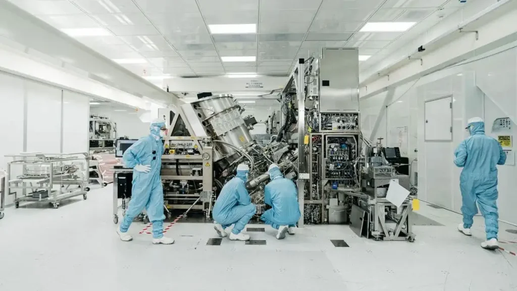
In a high-security facility in Shenzhen, Chinese scientists have achieved a milestone that Western sanctions were designed to prevent. A massive prototype machine capable of producing the advanced semiconductor chips essential for artificial intelligence and modern warfare is now operational.
Completed in early 2025, the machine is currently undergoing rigorous testing. It was constructed by a covert team that includes former engineers from the Dutch semiconductor giant ASML.
According to insiders, the group successfully reverse-engineered the complex technology behind Extreme Ultraviolet (EUV) lithography.
The Cold War of Light
EUV machines are the single most critical tool in the global technology race. They utilize high-energy beams of ultraviolet light to etch circuits onto silicon wafers. These circuits are thousands of times thinner than a human hair.
Currently, this capability is a monopoly held by the West. The smaller the etched circuits, the more powerful and energy-efficient the resulting chips become.
While China’s new machine is successfully generating extreme ultraviolet light, it has not yet produced functioning chips. However, the existence of the hardware suggests China is significantly closer to semiconductor independence than foreign analysts previously estimated.
A “Manhattan Project” for Chips
The development marks the climax of a six-year, state-led initiative to achieve self-sufficiency. The project is operated with the intensity and secrecy of a wartime mobilization.
Key operational details include:
- Secrecy: Engineers often work under aliases to hide their identities.
- Surveillance: Workstations are monitored by cameras to document the disassembly and reassembly of components.
- Isolation: Staff at sensitive fabrication plants are often restricted from leaving the site during the work week.
Huawei, the Chinese electronics giant, plays a central coordinating role. It manages a complex web of state research institutes and thousands of engineers. The project is overseen by the highest levels of the Communist Party’s Central Science and Technology Commission.
Technical Hurdles and Scavenged Parts
Despite the breakthrough, the Chinese prototype faces significant hurdles. Unlike Western commercial units, which are roughly the size of a bus, this prototype occupies nearly an entire factory floor. This increased size was necessary to generate sufficient power.
The most difficult challenge remains the optical systems. The machine fires lasers at molten tin 50,000 times per second to create plasma hotter than the surface of the sun. This light must then be focused by mirrors of unparalleled precision.
To construct the machine, China utilized a strategy of salvaging and reverse-engineering.
- Secondary Markets: Engineers sourced parts from older lithography machines bought at auctions.
- Restricted Components: The supply chain utilizes components from Japanese manufacturers obtained through intermediary networks.
- Talent Acquisition: The state launched aggressive recruitment drives, offering massive signing bonuses and housing subsidies to attract experts from abroad.
The Timeline for Independence
The government has set an ambitious goal to produce working chips using this prototype by 2028. However, those close to the project suggest 2030 is a more realistic target.
Even a 2030 arrival would defy Western expectations. Export controls imposed by the United States and the Netherlands were intended to keep China at least a generation behind in chip manufacturing. If this prototype succeeds, it could effectively remove the United States from China’s semiconductor supply chain entirely.


 Armenian Dram
 Ghana Cedi
 Gambian Dalasi
 Guinea Franc
 Nigerian Naira
 CFA Franc BEAC